By integrating micron-scale mechanical structures (e.g., cantilevers, diaphragms) with electronic circuits, we enable sensing and processing of physical signals – including acceleration, pressure, angular velocity, and acoustic waves in the physical world.
Leveraging materials like silicon photonics and thin-film lithium niobate, we achieve generation, modulation, transmission, and detection of optical signals.
In semiconductor chip manufacturing, cleaning processes run through the entire wafer processing flow, accounting for over 30% of steps. Technical difficulty increases exponentially with process node shrinkage. In semiconductor wafer manufacturing, photovoltaic wafer processing, and chip packaging/testing, precise removal of nanoparticle contaminants has become the "industry cancer" constraining yield.
MICVIO is China's leading provider of semiconductor AVI inspection and ultrafine particle removal solutions, dedicated to delivering high-quality inspection and cleaning solutions for chip manufacturing and packaging fabs.
When Chips Approach Physical Limits: Why Can a Single 0.1 μm Dust Particle Destroy a Fab?
Preface: The Yield Battle Enters the "Molecular Scale"
In a 2nm node transistor, the gate length accommodates a mere 10 silicon atoms. If such a transistor were scaled up to the size of a football stadium, a 0.1μm particle would be akin to a car wedged in the goal area—not merely blocking a channel, but directly altering the device’s electrical properties: leakage current surges by 10x, threshold voltage drifts by 50mV, and the failure probability of SRAM cells skyrockets by 1000x.
A daily arithmetic problem in semiconductor fabs: "How much yield is lost with each additional 50nm particle?" The answer ranges from 0.01% to 3%, depending on which process layer, which manufacturing step, and which type of device the particle lands on.
The core contradiction: As manufacturing processes approach the atomic scale, ultrafine particles have escalated from "accidental defects" to "systemic risks." Yield control has evolved from "process optimization" to a "molecular-scale battle." Meanwhile, the packaging stage—dubbed the "final mile" of chip manufacturing—faces growing particle contamination risks that have become critical variables determining yield and reliability.
Process Breakdown: In a Long Chain of 400 Processes, Where Are the Most Vulnerable to "Dust" Penetration?
1. Substrate Preparation (Ingot → Wafer)
Single-crystal pulling: In molten silicon at 1450°C, if carbon or oxygen is mixed in at a concentration of 10¹⁰ atoms/cm³, subsequent heat treatment will precipitate SiC or SiO₂ particles, which act as sources of dislocations.
Wire cutting + grinding: Powder shedding from diamond wires and residual SiC grinding fluid leave 20–80 nm scratches on the surface. Stress concentration at the bottom of these scratches easily leads to stacking faults during epitaxial growth, increasing the rejection rate of individual wafers by 5%.
2. Front-End-of-Line (FEOL)
Thermal oxidation/deposition: If SiO₂ particles from spallation of quartz components in the furnace tube land on the gate region, they are equivalent to embedding "micro-MOS" structures in the oxide layer, causing direct short circuits when gate voltage rises.
Photolithography: A 50 nm dust particle on a photomask, after 4× reduction exposure, still occupies 12.5 nm—sufficient to cut off a 16 nm metal line and cause functional failure of a single chip.
Dry etching: After polymer peeling in the chamber, CFₓ particles are bombarded by high-energy ions and embedded into the sidewalls of trenches, forming leakage channels, which leads to an exponential increase in yield loss.
Ion implantation: If photoresist residues are not removed, hydrocarbon particles will carbonize during annealing at 1000°C, forming "black silicon" cones. This causes a sudden 30% drop in breakdown voltage, requiring the entire batch of wafers to be reworked.
3. Back-End-of-Line (BEOL)
CMP for copper interconnects: Residual Al₂O₃ or SiO₂ abrasive particles from the polishing slurry at the copper/low-k interface increase RC delay by 5%–8%, leading to chip timing failures and a 15% rise in elimination rates during testing.
4. Packaging Process
The risk of particle contamination amplifies as manufacturing moves from "wafer-level" to "system-level." The packaging process involves multiple steps such as die sawing, die bonding, wire bonding, and molding, with more complex sources of particle contamination and more hidden impacts. Once a failure occurs, the rework cost is far higher than that of front-end processes.
(1) Die Sawing
Particle sources: Micropowder (1–10 μm) from diamond blade wear, residual coolant, and debris from wafer backside adhesive.
Failure modes: Particles in the saw street embed into the chip edge, causing stress concentration during subsequent packaging and increasing the risk of chip cracking by 30%. Large particles (>5 μm) scratch the chip surface passivation layer, triggering leakage or corrosion and resulting in 5%–8% yield loss.
(2) Die Bonding
Particle sources: Filler particles in die attach adhesive (e.g., Ag micropowder), peeled oxide layers on the substrate surface, and environmental dust.
Failure modes: Particles larger than 5μm cause "false bonding" between the chip and the substrate. After the Temperature-Humidity-Bias (THB) test, the shear force drops by 40%, and the failure probability rises exponentially. Nanoscale particles (<100nm) embed into the interface of the die attach adhesive, forming local stress concentration points, which lead to chip cracking during thermal cycle tests.
(3) Wire Bonding
Particle sources: Oxide layers on the surface of bonding wires, wear debris from ultrasonic bonding heads, and environmental organic contaminants.
Failure modes: Particles larger than 3 μm cause poor contact between gold balls and aluminum pads, reducing bonding strength by 50% and increasing early failure rates by 20%. Submicron particles (0.1–1 μm) induce electromigration at the bonding interface, leading to resistance drift exceeding 20% and long-term reliability failures.
(4) Molding
Particle sources: Agglomerated fillers in epoxy molding compound (EMC), residual release agent on mold surfaces, and airborne fiber debris.
Failure modes: Particles larger than 50μm induce internal voids in the mold compound, increasing the risk of chip delamination by 5 times during thermal shock tests. Nanoscale particles (<100nm) act as water vapor permeation channels, accelerating chip corrosion and causing a 10-fold surge in failure rates during HAST (Highly Accelerated Stress Test).
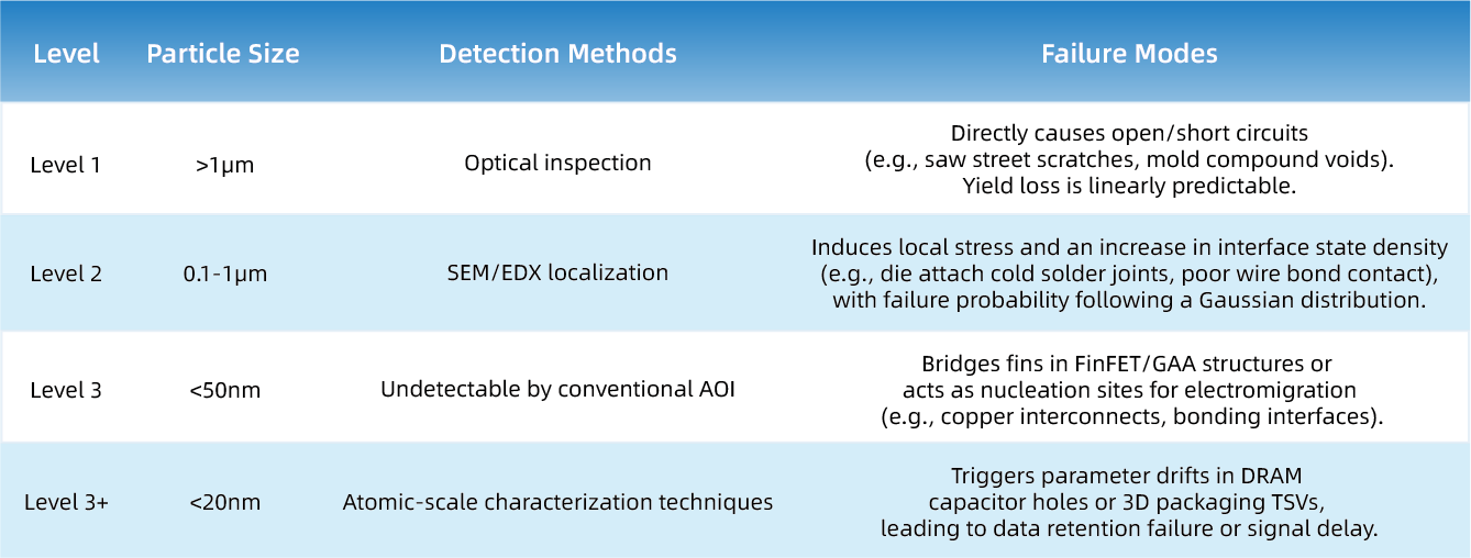
Pain Point Classification: From "Visible Scratches" to "Invisible Traps"
The chart analysis is as follows:
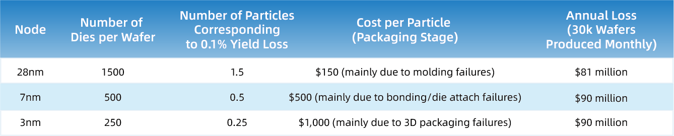
Economic Loss Model: Converting Particles into Dollars
The chart analysis is as follows:
Underlying Logic: In advanced manufacturing processes, although the cost of a single particle in the packaging stage is lower than that in front-end processes, its failure modes are more complex (such as thermomechanical failure and electrochemical migration), with rework costs accounting for 30%-50% of the total chip cost. If the yield ramp-up of a 3nm production line is delayed by 3 months due to particle contamination in the packaging process, the direct loss will exceed 1.5 billion US dollars (including allocated R&D costs).
Systemic Risks: When Particles Become "Amplifiers"
Process Window Collapse: The depth of focus in EUV lithography is only 100nm, and a 30nm particle can already cause pattern defocusing. In the packaging process, a 5μm particle can lead to an interlayer alignment deviation of >1μm in 3D stacked chips, rendering the entire chip scrapped. In the SAQP (Self-Aligned Quadruple Patterning) process, particles cause cumulative misalignment of patterns after four etching steps. In TSV (Through-Silicon Via) etching during packaging, nanoparticles result in excessive sidewall roughness, increasing resistance by 20%.
Reliability Avalanche: A 20nm particle in the Cu/low-k structure becomes a nucleation site for electromigration voids. In packaging interconnects, a 100nm particle can trigger incomplete micropore filling, increasing the probability of thermal cycle failure by 10 times. Nanoscale water vapor channels in the molding compound (caused by particles <50nm) shorten the chip's failure time in HAST (Highly Accelerated Stress Test) from 168 hours to 24 hours.
R&D Cost Out of Control: TSMC's 3nm production line investment exceeds 20 billion US dollars; if yield ramp-up is delayed by 6 months due to particle contamination in packaging, the direct loss will exceed 3 billion US dollars. Intel's 3D packaging technology (Foveros) suffered from interlayer void issues caused by particle contamination, prolonging the R&D cycle by 18 months and missing the market window.
Epilogue: Particles Are No Longer "Defects" but "Cost Amplifiers"
Beyond the 2nm node, transistors no longer have "excess space" to accommodate foreign atoms:
Physical Limits: The gate oxide thickness is ≤3 atomic layers, meaning any particle equates to a process catastrophe.
Economic Limits: A 3nm fab requires an investment of $20 billion, and a mere 1% fluctuation in yield can determine whether it breaks even.
New Packaging Challenges: Emerging technologies like 3D packaging and Chiplets expand particle risks from a "2D plane" to "3D space," where a single nanoparticle can trigger system-level failures.
Ultimate Challenge: As chip manufacturing enters the "angstrom era," ultrafine particles have evolved from "accidental defects" to "systemic cost amplifiers." Whoever can reduce sub-50nm unknown particles to a statistical zero across 400 processes (including packaging) will earn the right to define the next generation of Moore’s Law.
When Chips Approach Physical Limits: Why Can a Single 0.1 μm Dust Particle Destroy a Fab?
Preface: The Yield Battle Enters the "Molecular Scale"In a 2nm node transistor, the gate length accommodates a mere 10 silicon atoms. If such a transistor were scaled up to the size of a football stadium, a 0.1μm particle would be akin to a car wedged in the goal area—not merely blocking
2025/08/11
Industry News
Using a 1:10,000 scale diagram comparing hair to a gate, explain the "giant effect" of 0.5
PrefaceIn the nanoscale battlefield of semiconductor manufacturing, a "dimension rebellion" triggered by 0.5µm particles is rewriting industry rules. When we scale down the real world by a factor of 1:10,000, a strand of hair with a diameter of 50µm transforms into a 50-meter-tall steel
2025/08/11
Industry News
How Are Ultrafine Particles in Chips Generated? — A Comprehensive Reveal from Source to Failure
PrefaceAs chip manufacturing marches toward the 2 nm node, a 20 nm particle is like a "time bomb" with far more devastating consequences than one might imagine. At the 2 nm node, a single gate can only accommodate 12 silicon atoms; a 20 nm particle intruding into such a space is analogous