Cross-Border Global · Heart and Chip Connected - SEMICON China 2025, the annual grand event of the global semiconductor industry, successfully concluded recently. The exhibition gathered more than 1,400 upstream and downstream enterprises and attracted over 100,000 industry practitioners to participate in this grand occasion. As a leading domestic enterprise providing integrated yield improvement solutions, Oriental Crystal Source Microelectronics Technology (Beijing) Co., Ltd. showcased its full range of products and latest achievements at this exhibition, demonstrating the solid strength of China's intelligent manufacturing.
Technology Empowerment to Build Core Competitiveness
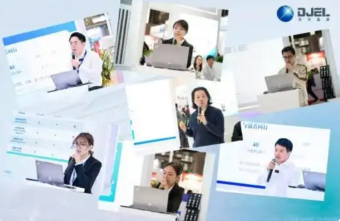
During the exhibition, Oriental Crystal Source formed a professional lecturer team consisting of senior engineers, presenting eight technical feasts for three consecutive days. The content covered core products such as advanced process domestic electron beam metrology and inspection equipment, computational lithography software, etc., and combined with the company's business direction, conducted multi-angle analysis on the development trends and technological innovation achievements of the semiconductor industry. At the same time, the combination of hardware precision and software collaboration demonstrated a complete technical closed-loop from equipment accuracy to data algorithms, and the product competitiveness was fully displayed in this exchange and discussion process.
In the speech, the technical team deeply explained Oriental Crystal Source's technological breakthroughs and application practices in the field of domestic yield management through detailed data and a large number of typical cases, enabling industry elites from all over the world to fully understand the level of domestic substitution and the overall development trend in this field. The on-site interaction and communication were active, and the high-quality and high-tech content greatly promoted knowledge sharing and ecological co-construction among upstream and downstream of the industrial chain.
Hardcore Product Matrix Breaks Through Key Technical Problems
In the past year, Oriental Crystal Source focused on core technical problems in the field, conducted in-depth research and development, continued to tackle key problems, and achieved a series of breakthroughs. During the exhibition, its iterative new products such as electron beam metrology and inspection equipment, computational lithography platform PanGen®, yield management platform YieldBook attracted many visitors. Among them, key achievements such as DR-SEM r655, PanGen DMC® (Design Manufacturability Check), and process optimization system PME (Process Margin Explorer) became the focus, and the staff conducted in-depth technical discussions on more technical details with upstream and downstream partners.
In terms of electron beam metrology and inspection, following the successful launch of DR-SEM r600 in early 2023, after two years of iteration, the latest generation of DR-SEM r655 is equipped with a new-type high-performance electron gun and optical inspection module, adopts an upgraded wafer transfer system and intelligent algorithms, and breaks through many technical difficulties to meet the application needs of domestic advanced process production lines. Based on the self-developed optical path and customized domestic deep ultraviolet laser source, its optical inspection sensitivity is increased to 20nm; at the same time, the complete system formed by CD-SEM equipment and ODAS (CD-SEM intelligent offline data system) is steadily approaching the level of internationally advanced equipment, laying a solid data foundation for the independent domestic substitution of the entire lithography process; and the new generation of EOS independently developed by Oriental Crystal Source has been successfully installed on its DR-SEM, CD-SEM, and EBI, taking the lead in achieving the application of domestic EOS in the field of high-end metrology and inspection, which not only helps to further improve product performance, but also provides key technical support for the independent and controllable industrial chain.
HPO Advanced Concept Drives Output of Innovative Achievements
Since its establishment in 2014, it pioneered the proposal of a full-chip Inverse Lithography Technology (ILT) solution based on CPU+GPU hybrid computing architecture. After 11 years of continuous iteration, the PanGen® yield comprehensive optimization platform formed on this basis launched PanGen®V5.0 version in December last year, which has been widely used in process research and development and mass production of domestic mainstream logic and memory chip manufacturers. In the display of the full series of tools around the software ecosystem, the core achievements are also particularly eye-catching, including the overlay mark optimization tool PanOVL, the verified PanGen DMC®, the 3.0 version of the yield comprehensive management platform YieldBook, the Chiplet multi-physics field simulation analysis tool PanSys, and the newly released PME.
It is worth mentioning that as another masterpiece of practicing the HPO concept following ODAS and YieldBook, PME has been fully deployed at the customer site, officially entering the product verification and evaluation stage, and is deeply integrated into Oriental Crystal Source's "equipment-data-algorithm" trinity, software and hardware collaborative yield improvement solution, becoming one of the strategic tools to break through the yield bottleneck of advanced semiconductor processes.
At the same time, the actual measurement results in a domestic advanced node FAB have shown that PanGen DMC® has reached the international advanced level in full-chip scale prediction indicators, and the difference between predicted results and actual ones is less than 1nm on over 99% of layouts. Key modules such as the technical core PanGen D2C® fast lithography feedback engine, potential hot spot detection based on PanGen D2C®, and hot spot model to improve adaptability have successfully integrated AI algorithms to realize intelligent identification of process hot spots, fully demonstrating Oriental Crystal Source's leadership and 前瞻性 in the integration of new technologies such as AI.
Facing the yield challenges brought by advanced processes, Oriental Crystal Source has been committed to providing more comprehensive and efficient technical support for domestic FAB customers, and has always adhered to driving industrial upgrading through technological innovation. A series of breakthrough achievements displayed around core products at this exhibition not only reflect its existing technical advantages, but also demonstrate its continuous innovative R&D strength. From electron beam metrology and inspection to computational lithography software, from point tools to system solutions, Oriental Crystal Source has gradually built a complete yield improvement technology ecosystem. In the future, Oriental Crystal Source will continue to increase R&D investment, deepen core technology research, promote China's semiconductor high-end equipment industry to move towards the high-end of the value chain, and inject strong momentum into the independent and controllable development of China in the global semiconductor competition pattern.
Source: Shiyan Evening News