Preface
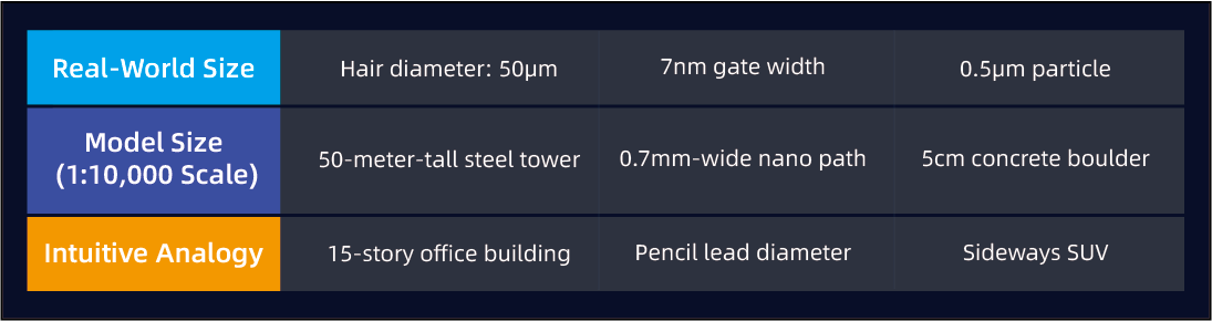
In the nanoscale battlefield of semiconductor manufacturing, a "dimension rebellion" triggered by 0.5µm particles is rewriting industry rules. When we scale down the real world by a factor of 1:10,000, a strand of hair with a diameter of 50µm transforms into a 50-meter-tall steel tower, while a 7nm transistor gate shrinks to a 0.7mm-wide narrow path. This "giant invasion" in the microscopic world stands as the core challenge confronting China's 7nm chip manufacturing.
Dimension Rebellion: Disaster Deduction at a 1:10,000 Scale
(1) Dimensional Mapping Between Reality and Model
This dimensional discrepancy is equivalent to forcing an elephant through a capillary vessel—when a 50-meter-tall tower stands in the center of a nanoscale city, a 0.7mm-wide channel simply cannot accommodate its existence. Although semiconductor 5nm etching equipment can achieve selective etching of 2,000-layer 3D NAND, it still struggles in the face of 0.5µm particles.
(2) Threefold Catastrophes of Particle Contamination
Total Occlusion Effect: A 5cm boulder precisely covers the 0.7mm channel, resulting in complete failure of the transistor. The FinFET structure employed in the Kirin 9010 chip features a channel length of merely 0.3µm, where any particle intrusion will lead to catastrophic consequences.
Economic Earth Earthquake: The Macroscopic Costs of Microscopic Disasters
(1) Wafer-Level Wealth Destruction
Each 7nm wafer contains 500 chips, with a single chip valued at approximately $15,000. When a 0.5µm particle causes a failure, it is equivalent to:
Crushing 500 nanochannels, resulting in a direct loss of $7.5 million. A 1% drop in yield translates to a $150,000 loss. Although some enterprises have mass-produced 28nm DUV lithography machines, in the 7nm process, the loss caused by a single particle is still equivalent to crushing 5 Rolls-Royce Phantom cars.
(2) Phantom Threats in Detection Blind Spots
The capture efficiency of existing optical inspection technologies for 0.5µm particles is less than 50%, which is analogous to:
Being unable to detect a 5cm obstacle from a height of 50 meters. It is necessary to rely on electron beam inspection equipment worth $2 million, with inspection costs accounting for 12% of total chip manufacturing costs. This dilemma manifests in the 7nm process as: An additional $3 million needs to be invested in defect analysis for every 10,000 wafers.
(3) Ultimate Challenges in Cleaning Processes

Traditional wet cleaning leaves a 0.21mm cleaning dead zone at the edge of the 0.7mm channel, which is equivalent to:
Leaving a 42-meter-wide hygiene blind area around a 50-meter tower. It is necessary to adopt megasonic cleaning technology, which increases the cleaning cost to $1,500 per wafer. This challenge has led to a 40% increase in the time required for cleaning processes in Intel's 7nm technology.
Technological Breakthrough: A Dimensional Revolution in Chinese Solutions
(1) Dimensional Breakthrough in Material Purity
Chinese factories producing 6N-grade ultra-high-purity metal targets (with a purity of 99.9999%) have captured 40% of the global market. Their precision reaches:
Impurity content <1 gram per ton, supporting 3nm chip manufacturing and prompting ASML engineers to recalibrate inspection equipment. This material revolution is equivalent to laying an absolutely flat "foundation" for nanoscale cities, reducing particle generation at the source.
(2) Dimensional Compression in Equipment Innovation
Chinese enterprises have delved into equipment innovation, developing prototype EUV alternative technologies through:
Carbon nanotube-cooled lenses and aspherical lens group designs, compressing equipment volume to 1/3 that of ASML’s. This innovation is equivalent to building a more precise "traffic control system" in the nanoworld, reducing the risk of particle contamination by 60%.
(3) Dimensional Control in Process Optimization
China’s semiconductor industry has formed a technological closed-loop with Prismo UHC equipment and PECVD systems, achieving:
A reduction in amorphous silicon deposition defect density from 10⁹/cm² to 10⁶/cm², a 20% yield improvement in advanced packaging substrates, and a reduction in 7nm process steps from 1,000 to 800. This precision enhancement is equivalent to upgrading urban road flatness standards from the meter level to the micrometer level.
Future Battle: Ultimate Deduction of the Dimension Game
When the process node advances to 2nm, the gate width will shrink to 0.2mm, at which point the relative height of a 0.5µm particle will expand to 25 times. This is equivalent to:
A 50-meter boulder crushing a 0.2-meter-wide country path, increasing the risk of particle contamination by 10 times and making cleaning difficulty grow exponentially. In the face of such challenges, China has adopted the strategy of "nurturing advanced technologies with mature ones," capturing 33% of the global market share in the 28nm process node to accumulate funds for technological breakthroughs. Among the 344 billion yuan of the National Integrated Circuit Industry Investment Fund Phase III, 5 billion yuan is specifically allocated to support the development of EUV technology. This strategic investment is equivalent to building a "flood control dam" in the nanoscale world.

Epilogue
In this nanoscale "war against giants," China’s semiconductor industry is building a defensive system through full-chain innovations in materials, equipment, and processes. "When we achieve excellence in the 28nm domain, those high-end technologies that once constrained us may instead become breakthroughs for us to redefine industry rules." This silent technological revolution is transforming the 0.5µm "dimension rebellion" into a stepping stone for China’s chip breakthrough. When the 50-meter-tall steel tower finally merges into the skyline of the nanoscale city, the golden era of China’s chip manufacturing may well begin.