Preface
As chip manufacturing marches toward the 2 nm node, a 20 nm particle is like a "time bomb" with far more devastating consequences than one might imagine. At the 2 nm node, a single gate can only accommodate 12 silicon atoms; a 20 nm particle intruding into such a space is analogous to parking an SUV sideways in a subway car—it would directly sever an entire signal line, inflicting catastrophic damage to the chip. So, how exactly do these ultrafine particles come into being? Below is an in-depth analysis spanning the raw material layer, environmental layer, and process layer.
In-depth analysis of the raw material layer, environmental layer, and process layer
(1) Raw Material Layer: "Inherent Risks" in Silicon Ingots
The fundamental raw material for chip manufacturing is the silicon ingot. However, during its production, the silicon ingot may already carry various "inherent defects," 埋下隐患 for the generation of ultrafine particles in subsequent processes.
Quartz crucible erosion: Under high-temperature conditions, the walls of the quartz crucible are scoured and subjected to thermal stress, causing 50–200 nm SiO₂ debris to mix into the molten silicon. Up to 10¹⁰ SiO₂ particles per cubic centimeter can be incorporated into the molten silicon; these particles will precipitate dislocations in later stages, severely impairing chip quality.
Crystal pulling vibration: During the crystal pulling process, microbubbles in the molten silicon form void clusters after solidification. These void clusters, during subsequent slicing procedures, lead to stress concentration at the bottom of scratches, resulting in a 1000-fold increase in the number of epitaxial stacking faults and significantly reducing yield.
Carbon and oxygen impurities: Silicon ingots may also contain carbon and oxygen impurities. During later heat treatment, these impurities precipitate into 5–30 nm SiC/SiO₂ clusters, reducing carrier lifetime by two orders of magnitude and exerting a severe negative impact on chip performance. It can be said that even before the silicon ingot is completed, the yield has already been significantly compromised by these "inherent particles."
The following are pollution sources in chip manufacturing and their impacts:
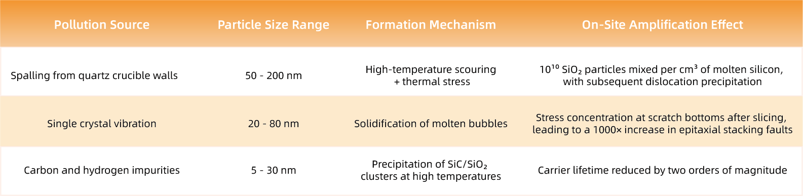
In the chip manufacturing process, different pollution sources generate particles with varying size ranges. Through their respective formation mechanisms, these particles exert significant on-site amplification effects, severely affecting chip quality and performance.
(2) Environmental Layer: "Invisible Threats" in Cleanrooms
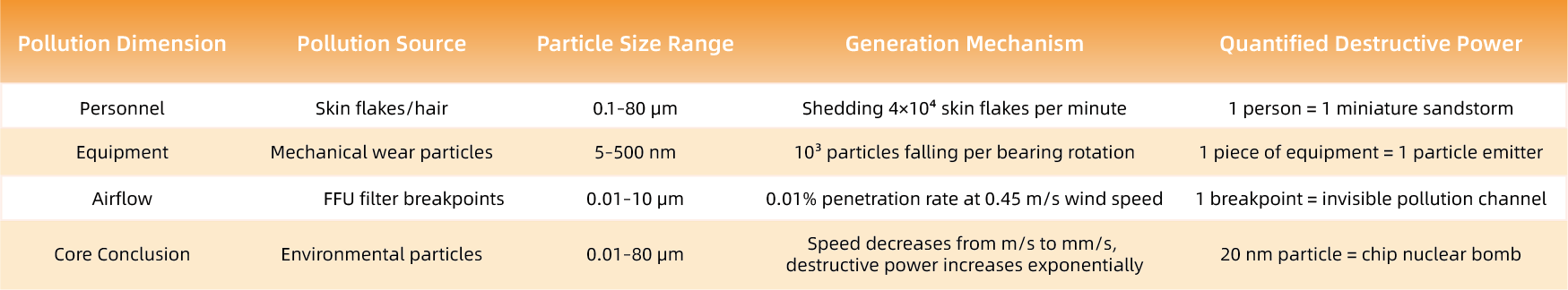
Cleanrooms are critical environments for chip manufacturing, but even in such settings, "invisible sandstorms" persist, continuously generating ultrafine particles.
Personnel factors: Personnel are a significant source of particles in cleanrooms. A single person sheds approximately 4×10⁴ skin flakes per minute, among which 0.1–1 μm particles have a certain probability of penetrating FFUs (Fan Filter Units). Despite a penetration rate of only 0.01%, these particles may still damage chips.
Equipment factors: Mechanical wear of equipment also generates a large number of particles. For example, bearings produce 10³ metal wear particles per rotation, with a peak particle size of 80 nm, posing a potential threat to chip manufacturing.
Airflow factors: Airflow control in cleanrooms is crucial, but in actual operation, when the wind speed is 0.45 m/s, the penetration rate of 0.1 μm particles is still 0.01%. This means that approximately 10 "bullets" may hit the wafer per second. Although their speed is much slower than that of traditional bullets, their destructive power increases exponentially as chip nodes shrink.
The following is a diagram legend (highlighting the contrast between particle size range and destructive power):
(3) Process Layer: "Relay Pollution" Across 400 Processes
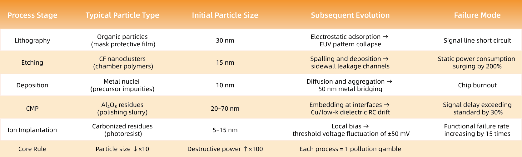
Chip manufacturing involves over 400 processes, and each process may become a "relay station" for the generation of ultrafine particles, continuously amplifying pollution.
Lithography process: During lithography, the mask protective film electrostatically attracts 30 nm organic particles. These particles can cause EUV pattern imaging collapse, leading to failure issues such as line breaks or bridging.
Etching process: Polymer 剥落 in the etching chamber forms 10–40 nm CFₓ nanoclusters. These clusters are embedded into sidewalls under the action of high-energy ions, forming leakage channels and severely affecting the electrical performance of chips.
Deposition process: During deposition, precursor impurities precipitate 5–20 nm metal nuclei. After being encapsulated by continuous thin films, these metal nuclei may cause gate short circuits, rendering the chip inoperable.
CMP (Chemical Mechanical Polishing) process: In the CMP process, Al₂O₃ residues in the polishing slurry have a particle size of 20–70 nm. These residues generate stress at the Cu/low-k interface, leading to RC drift and affecting the signal transmission performance of the chip.
Ion implantation process: During ion implantation, 5–15 nm particles from carbonized photoresist residues cause deviations in implantation dosage, which in turn lead to Vt drift, altering the threshold voltage of transistors and affecting the logical functions of the chip. Each process is a "particle relay"; as the chip node size is halved, the amplification effect of particles increases by 10 times.
The following is a pollution chain diagram legend (horizontal comparison of processes and particle evolution):
Physicochemical Amplification Chain: Evolution from "Dust" to "Disaster"
After ultrafine particles are generated, their hazards are further amplified through a series of physicochemical processes, evolving from tiny "dust" into a "disaster" for the chip.
Thermal budget: During a single rapid thermal annealing (RTA) process, 5 nm metal clusters can diffuse into 50 nm bridges, causing chip short circuits and rendering a large number of transistors ineffective.
Electric field focusing: The electric field intensity at the tip of a FinFET exceeds 5 MV/cm, and a 20 nm particle is sufficient to trigger breakdown, damaging the chip's insulating structure and making the chip inoperable.
Stress concentration: The stress concentration factor at the bottom of a scratch is greater than 3. During one temperature cycle, cracks may propagate by 100 μm, leading to crack defects in the chip and severely affecting its reliability and lifespan.
Economic Amplification Chain: Massive Losses Behind Particles
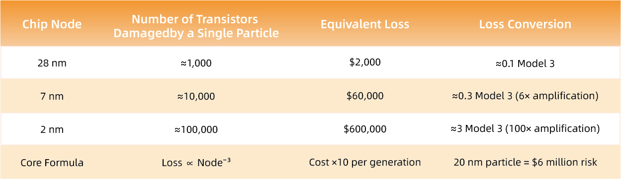
Ultrafine particles not only affect chip quality and performance but also bring huge economic losses to chip manufacturers. As chip nodes continue to shrink, the number of transistors that can be damaged by a single 20 nm particle grows exponentially, and the equivalent loss increases significantly. At the 28 nm node, a single 20 nm particle can damage approximately 1,000 transistors, with an equivalent loss of about $2,000; at the 7 nm node, it can damage around 10,000 transistors, equivalent to a loss of $60,000; and at the 2 nm node, it can destroy roughly 100,000 transistors, resulting in a loss as high as $600,000. Based on 500 chips per wafer and a unit price of $15,000, the loss caused by each 20 nm particle is equivalent to the value of a Tesla Model 3.
The following is a stepwise cost diagram (intuitively showing the cost of node transitions):
Invisible Blind Spots: Challenges in Detection and Root Cause Tracing
The detection and root cause tracing of ultrafine particles face enormous challenges, with many invisible blind spots.
The following is a diagram of detection capabilities (comparing theoretical limits with actual gaps):
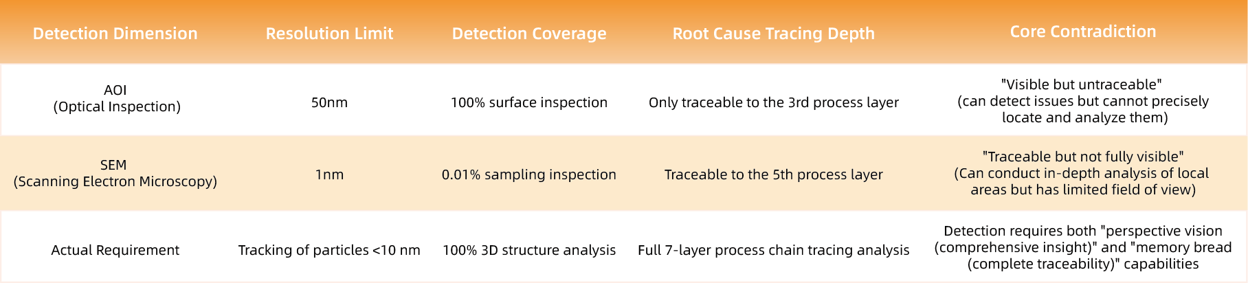
This table compares AOI, SEM, and actual requirements in terms of resolution, detection coverage, root cause tracing depth, and core contradictions, clearly demonstrating the characteristics of different detection methods and the gap with actual needs.
Epilogue
In the era of chip manufacturing beyond 2 nm, the gate thickness is equivalent to only 3 atomic layers, and any particle larger than 10 nm may instantly invalidate "atomic-level precision control." Ultrafine particles are no longer simple defects but a key factor determining whether Moore’s Law can continue to advance. From mines to packaging, 20 nm particles complete a "perfect crime" across 400 processes. Without needing weapons, their mere existence can make a $20 billion wafer fab record "abnormal scrap" in its financial reports. Therefore, in-depth research and resolution of ultrafine particle issues in chip manufacturing are crucial for promoting the continuous development of chip technology.